6/7 MHz clock upgrades and repairs
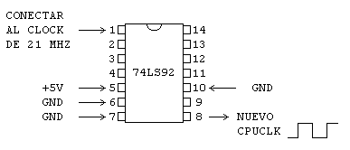
Repair for a MSX with broken clockoutput by Carlo Escobar.
Often the CPUCLK output from the v9938 becomes damaged (for example by instering cartidges with power switched on. Here is a solution to obtain an alternative CPUCLK.
6 MHZ opvoeren van Spectravideo en MSX 1,2 computers
Vrij veel toegepaste klokverhoging schakeling. Na veel updates universeel toepasbaar gebleken.
 Computer “on the double”
MCCM 86
Voer turboR op naar 40mhz
MSX Club Magazine 31
Turbo 7 MHz voor MSX Bouwbeschrijving voor klokversnelling naar 7 MHz met correcties
Turbo 7 MHz kit instructions how to build in.
(MSX CLub Gouda, Digital KC, MK Public Domain etc)
Software for MSX2+/7MHz/KUN Basic
With the MSX2+ and 7 MHz upgrade done by MK Public Domain (Digital KC) came some floppies:
MSX 7 MHz test program (MK Public Domain 1990)
MSX2+ demonstration program (MK Public Domain 1990)
KUN compiler demonstration programs and documentation
MSX Super Turbo
Designed and written by Alwin Henseler
Current version: 3.0 This page last updated: september 7, 1998
Status: finished (no real errors found since its last revision, in june 1995)
Please read this discussion also!
https://www.msx.org/forum/msx-talk/hardware/how-improve-msx-super-turbo-performance-msx2-hb-f9s-others
What is MSX Super Turbo?
The electronic circuit described below is a circuit that can
be used to switch the clock frequency of a Z80 CPU between 2
different values. This can be used to make a ‘turbo’ circuit in a
Z80-based system. It was originally designed for use in MSX
computers, but is probably suited for use in other systems as
well. In comparison with some known ‘competitors’, its main
advantage is the ability to switch between 2 entirely independent
frequencies. Both of these can be determined by using either a
quartz crystal (wide frequency range possible), or a suitable
external clock source. For both frequencies independently, any
combination can be used.
It can also serve as a direct 1:1 replacement for the well known
MSX 7 MHz. circuit. Most connections and the way it is built into
MSX computers, work just the same (but do note that this IS a
completely different circuit).
What can it do?
- It can make a MSX computer run faster
- It can be adapted (or used unchanged?) to make other
Z80-based systems run faster - Maybe you’re just interested to see how it works…
What can it not do?
- It cannot make any MSX run faster in all circumstances;
if the Z80 CPU inside the MSX runs faster, or is CAPABLE
of doing so, this does not automaticly mean that it will
be possible to LET it run faster, nor does it mean the
rest of the computer will work faster as well - It was specificly designed for speeding up Z80-based MSX
systems, so if you own a MSX that already has a more
speedy CPU (like a MSX Turbo-R): leave it be. If you have
another Z80-based system: it will probably work fine, but
you figure out how to build it into your specific
machine. For any other application: do as you like, I
won’t help you with it.
Design considerations
There have been several turbo projects for MSX in the past.
Most widely used is probably the 7 MHz. design, published in MSX
Club Magazine (numbers 31 (sept/okt. 1990), original publication,
and 34 (march/april 1991), minor corrections and improvements).
This turned out to be a reliable design, after the first
corrections and improvements, there were no real problems with
it, and has been used widely (MSX Club Gouda, MK Computers and
others).
Then there was this 6 MHz. project from the C.U.C. (Computer
Users Club). This design turned out to be rather ‘buggy’, one
improvement followed the other, and I doubt if it has ever been
perfected.
The main problem with the design of such circuits is this: the
Z80 CPU places some strict voltage level & timing constraints
on its clock signal input. Because of that, it is impossible to
use a simple electronic switch (like a multiplexer, or a few
logic gates) to switch between different clock signals.
The easiest solution is, to make use of some relation between the
signals that are switched between. In the 7 MHz. circuit, this is
done by using a 14 MHz. crystal base frequency, where an output
is switched between half, and a quarter of that (7.16 or 3.58
MHz, respectively), using a dedicated IC (Z8581 Clock Generator
Controller). I’m not sure how this is done in the 6 MHz. design.
Being busy at the time, buildings these things (7 MHz.) into
several MSX’s myself, more or less frequently, and having my own
MSX running this way, I kept wondering where speed limits
actually were (one always wants more). So, being not too clumsy
when it comes to hardware, I decided to make my own design.
‘Version 1.x’ consisted of a variable RC-oscillator, with its
timing coupled to a (slower!) 3.58 MHz. signal. It was absolutely
great to adjust the speed of one’s computer with a simple
variable resistor, but this solution turned out to be far too
sensitive to ‘environmental’ factors like temperature and
component variations, and was therefore quickly abandoned.
It was time to get back to the drawing board. Doing some research
on IC’s specially meant for this job, I found there were few to
choose from, their availability might be a problem, and the exact
way they worked, would largely remain a mystery. Not willing to
make any compromises on this, the demands for a new design became
clear:
- It should consist of ordinarily available parts, that
could be obtained just about anywhere, and at any time
(and probably low-cost), and, if not available, would be
easily replaced by other parts - It should, in principle, be able to switch between clock
signals that have no relationship with each other, so
that any suitable clock source can be used - The on-circuit clock sources should work independently,
each taking a quartz crystal as a timebase, or a suitable
external clock source, preferably without the need for
changes or settings in the circuit - The control signal used to switch the clock output,
should be a ‘don’t care’ (whatever, take an audio signal
for instance, or something at a higher frequency then
either of the clock signals involved) - It should preferably be ‘compatible’ with the existing 7
MHz. design, so that changes would be minimal when
replacing this with the new circuit
After having thought about this for a while, I worked out a
principle, that turned out to work so well, no need for another
design remained. ‘Versions 2.x’ consisted of the first practical
implementations of this, and having tested these for quite a
while, a thorough redesign was done (thus calling it version
3.0), which consisted of ‘cosmetic’ changes, mainly aimed at
making it more compact, leaving the principle unchanged.
With this latest version (designed in june 1995), all above
demands are met, it has been built into about a dozen
MSX-machines by now (several different types), and has stood ‘the
test of time’. Some improvements are still possible, I leave that
up to you, I didn’t feel a strong enough need so far (works fine
as it is)
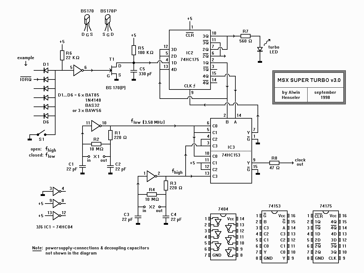
Circuit diagram
The circuit diagram (22 K, 1200 x
900 x 16 color GIF, actually black & white) contains the
complete circuit drawing, component values, and seperate
pin-layouts for convenience. Note that the
powersupply-connections of IC’s, and decoupling capacitors (100
nF ceramic between GND and Vcc of each IC) are not shown in the
diagram. As the designer of more circuits like this, I consider
these so ‘standard’, that I find such a diagram simply easier to
read without these.
Circuit description
In general, the circuit does the following:
It produces a Z80 clock signal equal to the ‘high frequency’,
until one of several inputs is activated. It then switches over
to a lower frequency (usually 3.58 MHz. for this purpose) as
quickly as possible (this is where most problems with designs
like this arise), keeps running at this lower frequency until a
certain delay (controlled by R5/C5) has expired, and then
switches back to the higher frequency. If in the mean while any
of the ‘switch-back’ inputs are activated, this delay starts from
the beginning again. Note that this is the ‘standard’
application, the frequencies used can be chosen freely, and it is
easy to modify it for using another way of switching between
these, or even to switch between more than 2 frequencies.
IC3 (a double 4-to-1 multiplexer) forms the heart of the circuit,
together with IC2 (a simple positive-edge triggered 4-bit
register). IC2 maintains a ‘current state’, and controls a LED
output signalling the current status. Its clock input is
triggered on the low-to-high transition, making sure that changes
occur only right after the ‘should be’ clock signal (IC3 pin 7)
has turned high (to meet Z80 CPU requirements). Its most
important output (pin 2) indicates the ‘desired ouput frequency’.
This is fed into multiplexer IC3. One half of IC3 is used
internally, to switch directly between the clock signals, which
is necessary to prevent the circuit from halting itself. At the
next low-to-high transition of this, a second output of IC2 (pin
15), following the first one, controls the actual switching of
the clock output. If these 2 controlling lines are the same,
multiplexer IC3 works as a simple buffer for the desired output
frequency. If the two controlling signals are different, which
may be understood as ‘circuit is in the process of switching
over’, the other multiplexer inputs (tied to the +5 V supply)
lengthen the high period of the clock output, needed for use by a
Z80 CPU.
The main advantage this setup gives, is that there is no real
difference between ‘switching from low to high speed’ and
‘switching from high to low speed’. This is treated exactly the
same, making the clock inputs fully interchangeable, and avoiding
problems that might arise, when it is switched again, while still
in the process of switching.
Crystal oscillators
The circuit contains 2 independent crystal oscillators. Each
of these can be set to a specific frequency either by connecting
a quartz crystal between the 2 connections, or by connecting a
suitable clock source to the connection marked “in”. No
quartz crystal should be present in this case.
The 2 oscillators can both use a quartz crystal, of the same or
different frequencies, 1 can use an external clock source, or
both, they can even share the same clock source (don’t know what
the use would be), this can all be decided for each specific use.
For both uses (quartz crystal or external clock) there are no
settings, or component value adjustments required.
If an external clock source is used, capacitors C1 or C3 will
simply add a small ‘capacitive load’, which any decent clock
source should have no problem with.
The circuit around X1 produces the ‘lower’ frequency (usually
3.58 Mhz), the circuit around X2 produces the ‘higher’ frequency,
usually somewhere close to the maximum speed the computer can run
on reliable.
Note: in some oscillator circuits like these, the parallel
resistor (R2 or R4 here) is connected directly between the input
and output of the inverter. In this design, this would probably
simplify the PCB layout. However, during testing, it was found
that this construction could cause startup problems under some
circumstances, leaving the oscillator in one non-oscillating
state. This might have been because of non-optimal component
values used, necessary to accomodate a wide range of crystal
frequencies without the need for any changes. In any case, the
slightly different construction used here solved this problem.
Speed control circuitry
Diodes D1…D6 form a discrete 6-input ‘OR’ gate (together
with R6), whose ‘output’ is fed into an inverter, which switches
‘on’ or ‘off’ FET T1. If switched ‘off’, this FET goes into a
high impedance state, allowing R5 to charge C5 to approximately
+5 volts. If switched ‘on’, it discharges C5, starting a delay,
after which the circuit switches back to the higher frequency.
The delay time is the time required for C5 to charge up to a high
input level for IC2, in this case about half the supply voltage,
so about 2.5 volts. The combination R5/C5 is calculated such,
that even the slowest components in the computer system can be
‘serviced’ at low speed, after an initial time they are accessed.
Switch S1 is used as a ‘7th input’, allowing the user to manually
switch back to the lower speed (usefull with audio applications,
or software depending on a particular CPU speed). Note that this
switch is connected between ground and the ‘other side’ of
D1…D6 directly, because it cannot produce a high level input
voltage. It may just as well be connected to one of the diode
inputs instead, or left out completely.
Component selection
C1, C2, C3, C4 = 22 pF
These capacitor values should be deviated from as little as
possible. The values are not critical, but required for the wide
range of operation this circuit offers (remember that this has
been extensively tested). If other values are used, chances are
things will work fine, but under some conditions problems might
occur. So please try and use the values indicated. Preferably the
common ceramic capacitors, or SMD counterparts should be used.
C5 = 330 pF
Together with R5, the value of this capacitor determines the
delay time, before the circuit switches back to the ‘higher’
frequency. With a CMOS type for IC2 (about 2.5 volts input
threshold), this delay time can be calculated using this
expression:
T = 0.69 * R5 * C5 (approximately, T in seconds, R in Ohms, C in
Farads)
With R5 = 100 K and C5 = 330 pF, this delay becomes about 23
usec, or about 82 clock-cycles at 3.58 MHz. This satisfies about
all MSX applications.
D1…D6 = standard diodes, any fast, small signal diode will do
(don’t use rectifier types). Better is to use Schottky types,
giving a lower voltage drop. Useable types include: BAT 85, BAT
82, 1N4148, 1N4448, BAS 32 (SMD). I used BAW 56, double-diodes in
SMD transistor-type housing (tiny little things), 3 pieces here.
IC1 = 74HC04 (6 inverters)
IC2 = 74HC175 (positive edge-triggered quad flip-flop)
IC3 = 74HC153 (dual 4-to-1 multiplexer)
All IC’s MUST be high speed CMOS types. IC’s like 74HCTxx,
74LSxx, 74ALSxx or 74Fxx will not do, because they will mess up
the output voltage levels, the duty-cycle of the output signal,
or the timing of the R5/C5 combination. Faster CMOS types will
probably be a GOOD replacement for any of the IC’s, as long as
types with CMOS compatible inputs and outputs are used (like the
74ACxx family). CMOS IC’s in the 4000 or 74Cxx family cannot be
used, simply because they won’t keep up with the speeds used
here.
IC1 would probably be well replaced by a 74HCU04 (unbuffered
outputs, this means a shorter delay, and a smaller amplification,
giving a more linear relation between input and output voltage,
like an opamp). In that case, it might be necessary to modify the
values of components used in the crystal oscillators, followed by
extensive testing. Advantage of using standard CMOS inverters
here, is that these can easily be replaced by other types, like
inverting gates.
R1, R3 = 220 Ohm
R2, R4 = 10 M Ohm
Used in the crystal oscillator circuits; use values as close as
possible
R5 = 100 K Ohm, determines delay-time together with C5
R6 = 22 K Ohm pull-up, may be anywhere between 10 times smaller,
or 10 times bigger
R7 = 560 Ohm, limits turbo-LED current, any value down to about
100 Ohm allowed. The presence of the inverse turbo-signal (IC2
pins 6 & 11) makes it possible to use a duo-LED (for instance
red/green), alternating LEDs, changing LED-display etc.
R8 = 47 Ohm
Used to supress ‘spikes’ on the output clock signal; try not to
change this value too much
In general, resistor values are non-critical, so ordinary carbon
types will do, slightly different values should be no problem,
and SMD or other types can be used as desired
S1 = ANY ordinairy switch; use the most ugly, big, or lousy
working ones you can find, if you want to. Any ‘bouncing’ effects
(call it ‘noise production’) when switching on or off is no
problem. Sometimes a switch with built-in LED is used, so that
the ‘turbo on’ indication is in the switch itself.
T1 = BS170 or BS170P (Field Effect Transistor)
This is probably the most problematic part of this circuit. The
BS170 and BS170P are the same thing, but with their connections
turned around 180 degrees (I hope they fired the sucker who made
that happen). An ordinary transistor (NPN) with series resistance
MIGHT be used instead, but I would strongly advise against it. By
the time this design was made, the BS170(P) was about the only
FET that was a) commonly available, and b) had the right
characteristics. There are probably several SMD types to choose
from now, which would be easier in construction. You could leave
out the inverter/FET section entirely, but this would require the
input signals to take care of discharging C5, which could
increase ‘switch-back-time’ in some cases. In this circuit, input
signal characteristics are ‘don’t cares’.
X1, X2 = quartz crystal, any ordinary type
The oscillator circuits are optimised for use with crystals in
the 3.58 to about 10 MHz. range, but have been succesfully tested
with crystals for frequencies as low as 2 MHz., and as high as 18
and 20 MHz. (crystal oscillators of this type will probably not
go too far beyond that).
Given this tolerance, most likely other types of crystals like
mini-types, or SMD counterparts can be used succesfully, but this
has not been properly tested.
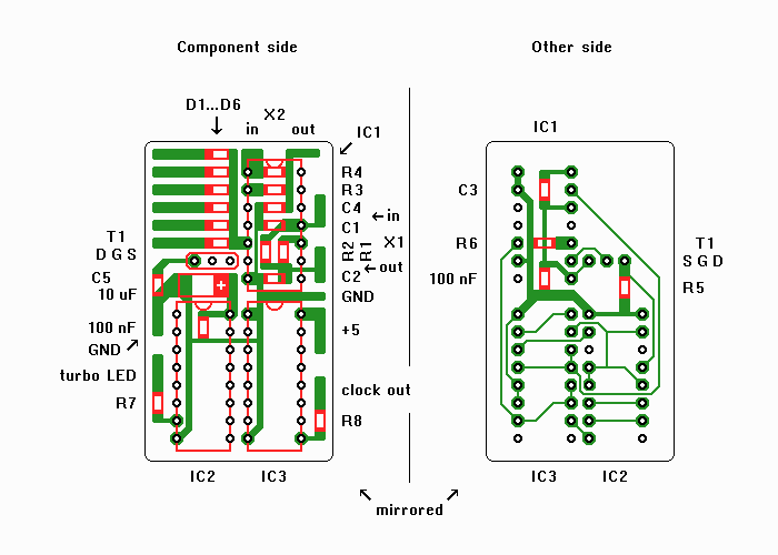
Decoupling capacitors
As in almost every digital circuit, every IC’s powersupply
should have a decoupling capacitor connected between the
powersupply-pins, with leads as short as possible. For this
circuit, a 100 nF ceramic capacitor should be used for every IC
(3 pieces), and a capacitor of 10 uF/10 V for the entire circuit.
SMD parts are preferred here, because these can usually be
located closer to the IC’s than ‘normal’ parts.
Note: in the PCB layout below, only 2 decoupling capacitors of
100 nF (SMD) are present. This is because one of these is placed
in such a way between 2 IC’s, that another one there would be
useless.
PCB layout
The PCB layout (12 K, 700 x 500 x 16
color GIF) is the one I used myself, when I last built these
things. Actual size is about 46 x 27 millimeters. Apart from IC’s
and transistor T1, all passive components used here are SMD
types, and most of these are placed UNDER the IC’s, or on the
other side of the PCB. It is included here only to save you the
trouble of making your own layout, in case you are able to
reproduce this one. If this turns out to be too difficult, or you
want to use another technique, you will have to make your own.
This circuit offers plenty of options to swap pins, to make this
easier. I will not include any instructions here on how to make
PCB layouts, or producing these things. Everyone making such
things will have to find his/her own way of doing this.
Copyrights
As the designer, I claim full copyrights on this circuit, and
especially where the principle it uses is concerned. At the same
time, you are free to use this information in whatever way you
like, for any purpose, as long as you observe these conditions:
- You may (re-)distribute this package unrestricted, as
long as all files in this package are included, in
unmodified form. If you wish to make any changes, or
convert this information into another form, then you
should do this by including your additions with these
original files, clearly stating what was added or
modified - If you make any publication of this circuit (for instance
by placing a modified version of it on a webpage of your
own), be sure to include information on how the latest
version of the original can be obtained (see below),
and/OR simply include this package - Should you incorporate this circuit in some product (in
any form whatsoever), be sure (in documentation with this
product) to give me credit for my part in it
That’s all I ask. Should these conditions be a restriction in
any way, or create difficulties for you, than please let me know
(see below).
How to obtain the latest version
On top of this page, there is a link named “this
page”, which should take you to a webpage containing the
latest version of this document. If for some reason this page
should become unavailable, visit one or more of the major
internet search engines, and enter “MSX Super Turbo”,
which should list a current location for this page.
Feedback / support
Personally, I have no interest anymore in further development
of this circuit as a turbo circuit for MSX computers. On the
other hand, I have no problem with answering any questions of
you, that might remain. And, if you want to make use of this
circuit on a commercial scale, I would be happy to help with
that.
Apart from that, I would be very interested, simply to hear about
your experiences with this circuit. What you did to get it built,
where it was built into, how it works for you, what problems you
encountered etc. If you have any additions to this circuit, like
suggestions for improvements, or other applications, I will
include these on my webpage.
Alwin Henseler