A set of documents and emails Joseph Zbicia received from Karl Guttag regarding the TMS9918 and related VDP products, as well as some documentation on the TI Home Computer lines (TI-99/4A and related products) and 9900 family CPUs. It seems he’s gotten a few inquiries over the years about the VDP and friends. 🙂
There is a lot of interesting information, including how to decode the VDP’s colors, how the 9918A’s Graphics II mode came about, and so on.
- 1981 Home Computer Comments on 9995.pdf
- 99000 (Alpha) Misc Documents.pdf
- 99-4 History By KG in answers to Matthews Questions.doc
- 9985 Instruction Cycle Times.pdf
- Message on Modification to 9918 from 1982.pdf
- 1978 9918 Master Timing by Serigio Maggi.jpg
- 1978 Pattern And Sprite Processing.pdf
- 1980 TMS9918 Advertisement.jpg
- 1981 VDP Debacle Memo by KG.pdf
- 1982-12 Coleco in Consumer Reports.pdf
- 198x Super Pattern Graphics Mode (Mode 2).pdf
- 198x VDP DRAM IF spec memo.pdf
- 1977-10-18 9918 DRAM IF Proposal 300dpi.pdf
- 1979-or-1980 TI59 Calculator to 9918 Interface.pdf
- 1980 Arizona Technical Symposium Draft.pdf
- 1981 Message explaining why no multi-color in text mode.pdf
- 1982-03 Home Computer Request for Mods to 9995 and 9918.pdf
- 1982 Home Computer Feature Requests.pdf
- 1982 or 83 Presentation by KG on VDP problems .pdf
- 1982 TI Europe Proposal for 9929A Improvements (inc. External Video).pdf
- 198x External Video by KG.pdf
- 198x External Video by Pete Macourek.pdf
- 198x Technology-Transistor Trends.pdf
- SPPA004A 9928-29 9118-28 Interface to Monitors.pdf
- attachment (US Patent 4,243,984 PDF file).
Thanks go to Karl Guttag for providing this great material. Joseph Zbicia for publishing.
Original location page of Joseph Zbiciak
First Set of Documents Karl Guttag
I have the documents I sent previously in 3 sets that I was scanning while watching TV. This first set was in response to a bunch of questions Matthew had about my work on the 9900 family processors. Literally within a day of your email, I got an email from Matthew and then he responded with a list of questions about my involvement in the 9900 family. In answering those questions, it hit me that I had a lot of old documents on the 9918/9995/99000 that were sitting in boxes that some others might enjoy for historical purposes.
If you read the 99-4 History by KG MS-Word document first, it will put into context this first set of documents. Also this document gives a good bit of information on the 99/4 development from my point of view (that of one designing the 9918 and later architecting/designing 9900 compatible processors that were slated to go in future 99/x products). At the start of the 99/4A, I was just a young new hire at TI. In a year and a half, I went from a new hire out of college to the head architect of TI’s next 16-bit microprocessor. I had a tremendous amount of responsibility as head architect, but not a lot of clout on the direction of the product line as a very young engineer.
Karl
The 9918 was the first chip I worked on at TI and so it has a special place in my heart. After the 9918 and after the 9918 was complete, just a year and a half out of school, I became the chief architect of the 9995 microprocessor that was going to be using in the 99/2 and the 99/8 but they cancel the family before those products went to production. So I almost designed both the graphics chip and the CPU of the family.
Related to your hobby, at TI I hired another person Joe Zbiciak who’s first computer was a 99/4A when he was about 8 years old. Joe is extremely bright and his hobby is making software games for Mattel’s Intellivision emulators (see: http://spatula-city.org/~im14u2c/intv/ ); he also had one of those as a kid. Mattel was interested in the 9918 for Intellivision, but we couldn’t sell it to them because the Home Computer Group was suppose to need so many 9918 of them for the 99/4 (pre A), but as it turned out the Home Computer was delayed and Mattel went with an older less capable chip.
We were about the cancel the whole 9918 program when Coleco came in with Colecovision and the TI Home Computer took off while at the same time the MSX computer in Japan (the “MS” standing for Microsoft which had a short lived joint venture in Japan) started selling big time using the 9918.
Not many people know this but Nintendo’s original game system was based on a register level compatible superset clone of the 9918 done by Yamaha. Nintendo had developed games for the Colecovision, including Donkey Kong, and they moved this to their new game system.
In the early 1980’s, I was a big fan of the show “Connections” by James Burke was a great program that showed (albeit loosely sometimes) how there are a series of connections between inventions and often times the person that becomes famous may have just been the one person that added one key improvement on top of a bunch of other ideas/inventions. I am a bit of a computer history buff (but less so as I go married and had children).
One document has the 9985 instruction cycle times. This is very rare and unpublished since that part never went into production. Note that we ran with divide by 2, 3, or 4 of the “crystal frequency” to get the clock cycle time on various CPUs that TI did at the time and this is a source of confusion. In these documents you have to look for the “state rate” or “machine cycle time” but sometimes documents will talk about the crystal frequency. This document will give you an idea of the performance of the 9985 relative to the 9995, for example a 16-bit register to register Add on the 9985 took 10 cycles were it took 4 on the 9995 (and the 9995 clock rate was higher). In particularly compare this document to those on the 9995.
I also came across some miscellaneous communication between the Home Computer group on the 9995 and the 9918 modifications that became the 9118. On the message I sent the “TO:” list were all in the Home Computer group.
Lastly there are some performance comparisons between the 99000 (internal TI code name was Alpha), the 9995 (which was first call the 9985A but was later changed to the 9995 which other than for byte operation took the same number of cycles for the most part), the 9900, the 8086, 68000, and Z8000. Note that we didn’t even bother comparing to the 9985 as it was so poorly designed (but keep the code names straight because the 9985A became the 9995 and was totally different than the 9985 with no “A”).
Also in your last message you said you hoped I got a good raise off the 99000. Actually I was pretty poorly paid through the 99000, but soon after the 99000 was finished they made me the youngest “Senior Member of Technical Staff” and more than doubled my salary in one pay raise (I also skipped over several job gades). In my first 4 years at TI, I had gone from one of 6 engineers on the 9918 (although I got do work on much of the architecture because the engineers other than Pete Macourek primarily did circuit design) to being the lead architect of two 16-bit microprocessors.
From: Karl Guttag Subject: Second Set of Documents
This is the second set of documents. They particularly related to the 9918.
I knew I had a cache of materials on the 9918 history that I hadn’t found and tonight I found were quite a few documents had been stored. I figured I should scan them so they never get lost again. I have a lot more stuff that I may scan later.
The attached are:
- One slide/foil hard copy from a presentation I gave around 1982 or 83. It should be noted that I finished working full time on the 9918 in 1978 or 4 years earlier, but kept up with the 9918 as a pet project. In late 1978, I was put on trying to debug the 9985 and then late in 1978 I became the lead architect of the 9995 (aka 9985A). In late 1979 I started on the 99000 (aka Alpha) and finished it in 1982. It talks about the checkered history of the 9918. What many don’t realize is that TI came very close to cancelling the 9918 program in 1980 or 1981. They would have kept making it for the Home Computer but withdrawn it from the general market. Mattel showed Interest in the 9918, but the Home computer projections were so large that that TI was afraid to commit to Mattel in case there were not enough chips. As it turned out Mattel sold a lot of systems and Home Computer didn’t. Imagine if a system with Colecovision’s capability had come out 2 year earlier.
- Just a year or so after the 9918 was almost withdrawn from the market, in 1982 Colecovision came out and about the same time the 99/4A took off. Attached is a Consumer Reports article. The 9918 was fully function in 1978 and thus was about 4 years old. It is amazing that it was still the best video game chip on the market.
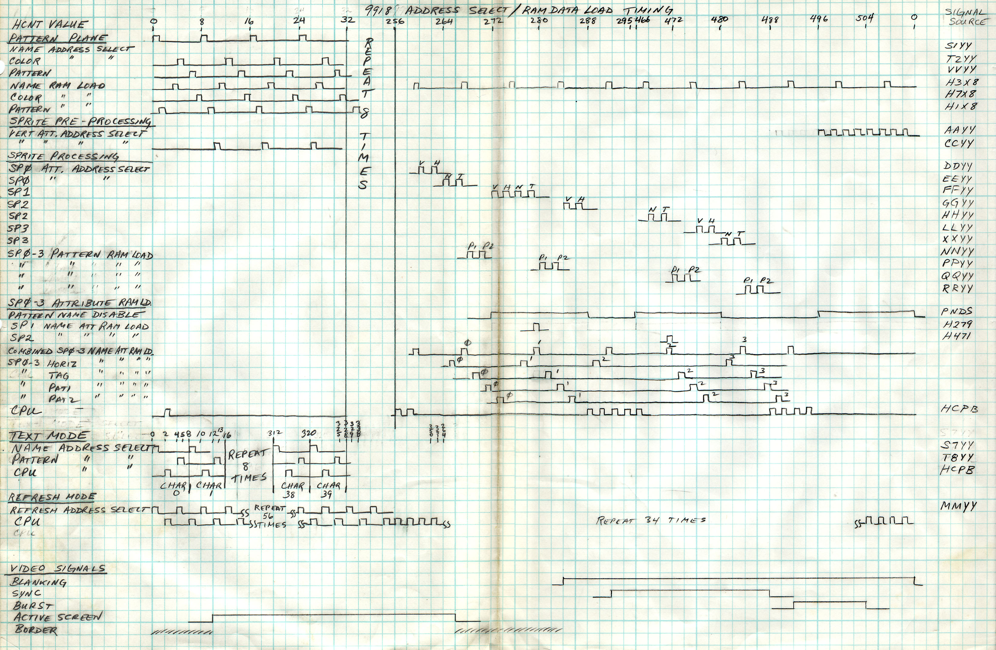
- The large (B-Sized 11×17 inch) Timing Diagram was an original one hand drawn by Sergio Maggie. Sergio designed all the high speed clocks on the 9918 and had a programmable logic array (PLA set of NOR gates) that generated a bunch of signals that kicked off various events. The PLA had inputs for the various modes like Text Mode, Graphics Mode, and the like. You might note that there are clock cycles across the top that jump from 295 to 466; this was a common type of “cheap trick” to save some logic, the horizontal counter was designed to with signal that made it jump to 466 after 295. Note, I’m not sure but we may have changed the total counts per line so this may not line up with later versions of the 9918/9918A/9118.
- A few pages that I wrote up on the Pattern and Sprite processing. The “neat” writing on the bottom of the page I think is Sergio’s, the messy hand print is mine. You will note that these diagrams found their way into the documentation, but I don’t think I was the first one to write up the addresses this way.
- An early 1980s memo I wrote on the 9918 memory interface. As I told you earlier, the 9918 was originally defined “little endian” but the documentation did a cosmetic swap to big endian. I must have gotten at least 6 calls from support people trying to help a customer that had laid out their PC board wrong. You will note in later editions of the 9918 family documentation there is an explicit table and warning as to how to hook up the DRAM interface.
- Next is an early 1980s memo I wrote on how to put in a “Super Graphics Mode” which I think ended up being Graphics Mode 2. Note it only took 50 transistors! I was trying to beef up the capability of the 9918 a bit but there was not a lot of support. Unfortunately as I discussed in my prior document, there were not enough memory cycles available to support a simple bit mapped mode.
- Next is a memo I wrote in frustration to Wally Rhines (then VP of our group and later/today CEO of Mentor Graphics) in 1981. It is a rather blistering memo. I was working on the 99000 at the time but still gave occasional support to the 9918. I should add, I was not the only person helping keep the 9918 alive but I was frustrated that it was still the best chip available and it had next to no sales after 3 year. That all changed about 1 year later when Colecovision and the Home Computer went to high volume for Christmas of 1982 and 1983.
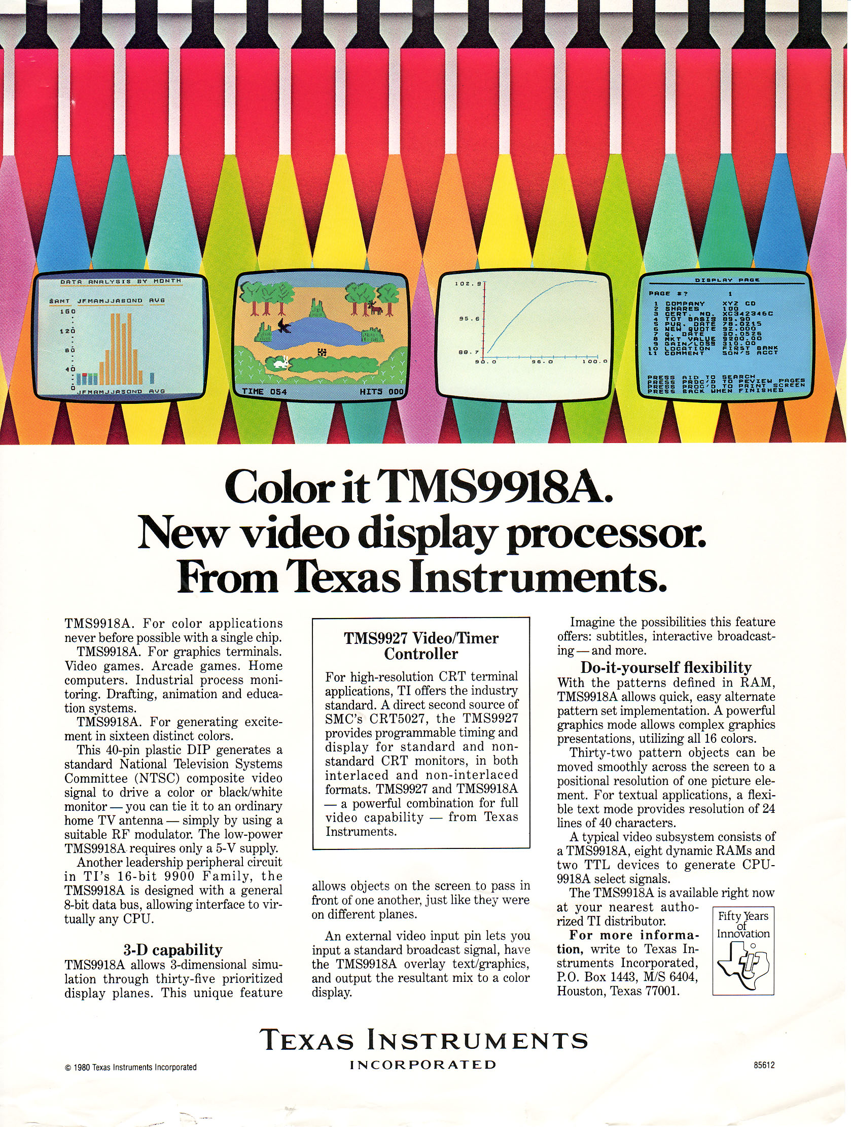
- Attached is an advertisement that is mentioned in the 1982 or 1983 presentation (item #1 above). Basically TI was only selling the 9918 to industrial control system companies rather than to games companies. The reason marketing gave me was that Industrial Controls is traditionally where the 9900 family sold the most. I remember distinctly telling them that the 9918 marketing “Was like a drunk looking under a streetlamp for his keys, and when asked if that is where he had dropped his keys, the drunk reply ‘no, but the light is better here.'”
I would consider the ones above to be of 9918 historical interest. I found a number of other documents including ones on video overlay and Dual VDPs in a single system. Maybe I can send them at another time.
From: Karl Guttag Subject: Third Set of Documents
Attached is another set of 9918/9995 Documents and Home Computer and some other “history” documents. I have tried to make the titles somewhat self explanatory, but there are a few explanations below.
Among them is the hand written timing diagram that I wrote for the 9918 DRAM interface for putting CPU write data on the Address bus. I saved this document because a couple of other engineers thought it was not possible without a lot of other external buffers or taking an extra cycle to turn the data bus around. I had only been at TI 4 months and this made a bit of my mark as a problem solver. This minor breakthrough was very important to give us enough CPU accesses.
There are several different articles on External Video.
There are documents on the Home Computer requests for modifications and enhancements for the 9918 and 9995.
I also included the documentation I wrote up on a TI-59 magnetic card based calculator interface to the 9918. I think I did this in 1979, because some of the documents are on English “A” size paper (slightly different than 8.5×11-inch) which would suggest that I had returned from England in 1979 with a pad of paper. I had a cable that would plug into the ROM expansion slot in the TI-59. I still have the electronics in the garage (but it hasn’t been fired up for 28 years).
From: Karl Guttag Subject: RE: TMS9918
The simple answer to your question is that it was all about cost and ease of implementation. The Home Computer Group provided a lot of the input on how the color was done on the 9918. It was driven by trying to implement the NTSC type signal.
The Video Color Palette on the 9918 was very limited and hard wired. I don’t know how much you know about NTSC signal, but the basics are that there is a color burst at ~3.58MHz. The 9918’s input clock was ~10.74MHz or exactly 3 times the color burst reference. In NTSC the intensity is the average DC level over a period of time, the color/hue is given by the phase shift from the burst reference of an AC color signal that is at 3.58MHz only shifted, and the saturation (amount of color) is given by the amplitude of the AC signal at ~3.58MHz.
To get color on the 9918, there was a simple resistor tap network. A very long resistor (made out of a long zigzagged polysilicon resitor)was tapped to give various voltage levels. The 10.74 MHz meant that we could get 6 basic color phases/hues just by running a shift register of the 10.74. This shift register was used to control the signals that controlled the tap point on the resistor. A pair of tap points was select, the further apart the tap point were, the more saturated the color and the average of the two tap points set the intensity/brightness (for gray, the two tap points would be the same).
Between the 6 basic phases, we could “tweak” the color by putting in a slow buffer (putting in smaller transistors into a buffer) after the shift register to slightly delay the tap point selection and thus shift the hue slightly. As I remember it, the Home Computer group picked the colors and I remember the colors being adjusted at least once after the first silicon to adjust a few of the colors.
Figures 10 to 12 in the attached patent show how it worked (and Figures 10 and 11 were pretty much taken directly from the schematics).
On the 9928 and 9929 that provided YCrCb, we did a pretty similar D-to-A technique (resistor with tap points) only there were 3 simpler ones since we only had to pick a point for the Y, Cr, and Cb for any given color. With the resistor we had a pretty wide choice of colors.
This is all pretty primitive compared to the latter color palettes also known as RAMDACs which had RAM based color lookups to a more flexible D to A converter. The RAMDACs was a term used by Brooktree and one of the founders of Brooktree, Jeff Teza worked on the Home Computer (it was his first job out of School. I also helped defined several color palettes at TI.
Hopefully the above plus the attached patent helps. If you have any questions, feel free to ask.